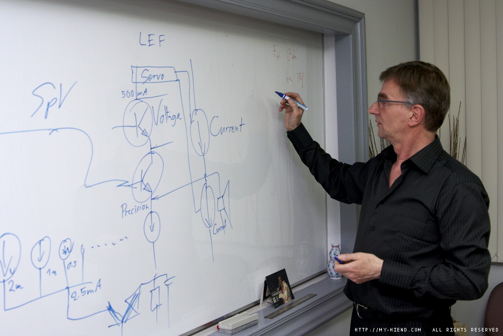
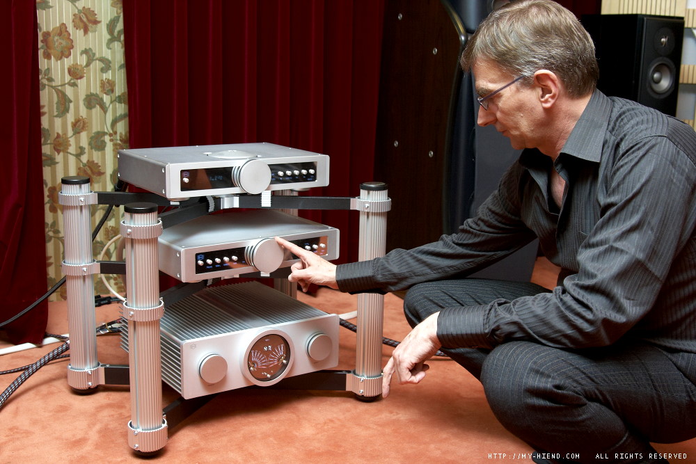
在代理商的會議室中,Michael就像教授般的跟學生(我)”重點式”解說B.M.C產品的獨特設計想法,從輸入線路、輸出線路、唱頭放大、DAC、轉盤、唱放,甚至電源供應都一一解說,一下子一小時就飛快的過去了,雖然我沒辦法完全吸收,但我會盡可能說明我所理解到的,若有錯誤之處也請大家不吝指正。在訪談最後,Michael也提到其正在進行錄音,講到這,當然跟我就很有話題了聊啦!
真材實料,具有很強know how的B.M.C
這張圖就可看出我是真的像在上課一樣喔!
B.M.C是CANDEIAS齊下的一個品牌,CANDEIAS是一家歷史悠久的音響設計公司,如CEC就是他們所設計的,創辦人為Carlos Candeias,在兩年前慕尼黑上有看到他,會說流利的中文,去年音響展也有來台,B.M.C是CANDEIAS自有品牌,想當然爾,是最能實現與應用CANDEIAS技術理念精華的產品,也難怪上市時間不長,卻已有各地許多的代理商了。
這次Michael來訪,主要是說明B.M.C擴大機最重要的特色與技術核心,也是為什麼B.M.C的聲音會出色的原因,這些技術的主要重點就是CI、DIGM與LEF。
CI (Current Injection):低阻抗的訊號輸入會使訊號以原來的電流經過放大線路,直到到達喇叭所需的輸出電壓。所有的B.M.C產品都可與CI輸入搭配,擁有最好的聲音可能。
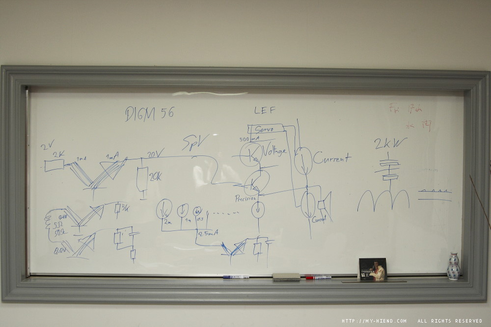
DIGM (Discrete Intelligent Gain Management):這個是非常特別的一項技術,只有在喇叭輸出電壓的這個地方,增益(Gain)會精準的對應到所調整的音量,也就是說是透過增益的調整來進行音量大小的控制,這樣的好處是可以避免一些不必要的放大導致訊號衰弱下來,更少的放大就會擁有更少的失真與噪訊,音樂最會有更自然的品質。(傳統擴大機的放大倍數很高,其實是不需要這麼高的倍數,變反過來將原本的輸入訊號降下來,從下面這張圖就可很清楚的看出來差異)
LEF (Load Effect Free):LEF輸出級調整輸出電壓到喇叭所需要的值,喇叭不需要負責調整,因此信號電晶體非常的重要,必須在一開始就能避免失真,LEF即使在高功率輸出也能維持單端的運作,也因失真減少,聲音會更為自然。將電壓與電流輸出分離的設計也可避面相位轉動的問題,聲音表現甚至比A類還要更清楚。
除了以上3個特點外,B.M.C 超大的2kW環型變壓器提供了超額設計的電源供應。
另外B.M.C的CD轉盤使用皮帶驅動,Michael表示這是讓CD轉動速度最能穩定的方式,就像黑膠唱盤一樣,也是能有效降低jitter的設計,唯一會讓速度變動的時間就是在換曲目的時候,可是這時候沒有音樂,當然就沒有影響了。
Thanks a lot for your therad about BMC Audio! I can only read a little, and the google translation is not always correct… It is even harder to contribute something to your website, because my written Chinese is ZERO. But may be I can write to you by email, and step by step offer a little more information. As our technology is really new and unique, it is difficult to understand – even for people with a solid technical background. May be you can help me translating my comments to Chinese and publish them?
(以上翻譯略,就是Michael感謝MY-HIEND的報導,也希望我幫忙把他進一步解釋的部份翻成中文給大家,BMC的理論非常新與特別,就算是讀電子的可能也不太容易懂)
“Accuphase’s AAVA circuit has nothing to do with our BMC design – much to complicated. AAVA has an input buffer, a V-I converter stage, a current addition and finally an I-V converter stage with a feedback loop and gain.
Accuphase AVVA的線路跟BMC不同,BMC複雜多了,AAVA有輸入緩衝,一個V-I轉換級,會增加電流,最終會有一個回授與增益的I-V轉換級。
To understand our approach it does not need to think that complicated.
瞭解BMC的方法不需要想得這麼複雜
CI input with DIGM volume control is a 1-stage amplification. The volume
control is just done with resistors (switched by transistors) at the output of this stage. After this gain adjustment there is no more voltage amplification. This means: The volume control happens at the voltage level of the speaker output.
使用DIGM音量控制的CI輸入是一級放大,音量控制是由輸出級的電阻(電晶體轉換)來處理,在這增益的調整後沒有任何電壓的放大,這意味著音量控制發生在喇叭輸出的電壓水平。
The only thing in common with the AAVA is: we have a potentiometer in the DAC1, a CPU reads out the position of the volume knob and translates it to a digital word, then this word is sent to the amplifier AMP S1 (or M1) by an optical connection. In the amplifier the digital word is used to activate some of the transistors of the DIGM to switch the required resistor (or combination of resistors).
與AAVA唯一相同的是,在B.M.C DAC1中,有個分壓計,CPU可以知道音量選鈕的位置將其變成數位語言,然後透過光纖將其發送到擴大機AMP S1 (或 M1)。在擴大機中,這些數位語言會啟動DIGM的電晶體來轉換成所需的電阻 (或將電阻組合)
It is a 1-stage design. The ouput of this stage is a current source. The gain is adjusted by the termination of this stage with a resistor, thus setting the I/V conversion.”
這是一級的設計,在這級的輸出的來源是電流,增益是在這級最後由電阻來調整,就是I/V轉換
I hope this helps a little for a better understanding of DIGM.
I’ll follow up with more explanations…
Let’s go on with the special BMC technology.
來說說BMC特別的技術
Please understand our basic difference to most of the circuits: We don’t use operational amplifier designs for audio, and we don’t use any kind of negative global feedback loop for the audio signal. Thus comparing our approach with AAVA or gain cell makes no sense.
請瞭解我們跟大部份線路根本上不同的地方:聲音方面我們不用運算放大設計,聲音訊號也不用任何種類整體負迴授迴圈。因此跟AAVA或是Gain Cell比較是沒意義的。
My last email was about the DIGM. At DIGM we are at the speaker terminal voltage (電壓 ), but there is not the power (電功率) and specifically not the current (電流) to drive a speaker. Thus we need a buffer stage to provide the current.
我上一封Email關於DIGM,在DIGM下,達到喇叭終端的電壓,不是電功率,特別是指不是電流來驅動喇叭,所以我們需要一個緩衝級來提供電流。
In all usual power output stages one pair (or more pairs) of transistors has to handle the signal precision, the voltage and the current. As this is quite demanding, it usually failes in precision – and needs a feedback loop for reducing distortions. There is even the difficulty to handle complex loads, like real world speakers, as they are partly inductive and / or capacitive. This means signal voltage and signal current are not allways in phase. Means: There are moments when the voltage is 0, but there is still a demand for current. How can this be handled by a transistor having the task of caring for the right voltage AND the right current?
在所有一般的功率輸出級,一對或多對的電晶體必須處理Signal precision,就是電壓與電流,且需要回授迴圈來減少失真。處理複雜的阻抗是困擾的,就像喇叭一樣,部份是電感或電容。這意偽著訊號的電壓與訊號的電流通常不是相位一致。也就是說,當電壓為0,但還是對電流有需求,那麼一個電晶體如何處理正確的電壓對應正確的電流?
LEF is different. It is like giving different jobs to different people.
LEF means Load Effect Free. Means: The LEF signal transistor (responsible for the signal quality – the precision) has neather to handle the voltage, nor the current. Thus it needs “assistants”: A cascode transistor to handle the voltage changes, plus a pair of current sources to deliver the required current.
LEF是不同的,他將不同的工作給不同的人,LEF意思為Load Effect Free。也就是LEF訊號電晶體(負責訊號的品質- precision)不是處理電壓或電流,他需要”助理”,一個cascode電晶體處理電壓的改變,加上一對電壓來源來提供所需的電流。
This circuit design is intended to avoid distortions by a new and unique design, instead of a later correction by feedback.
這樣全新與特別設計的線路用來避免失真,而不是後來回授的修正。
Beside of avoiding distortion, the independend handling of voltage and current by different “experts” makes handling inductive or capacitive loads just a piece of cake: The LEF signal transistor together with the cascode transistor care for the correct voltage. The current servo circuit with the current sources deliver the required current, not “knowing” anything about the voltage, just keeping the current through the LEF signal transistor constant.
除了避免失真外,由不同”專家”獨立的處理電壓與電流,讓處理電感與電容阻抗變成非常容易的事。LEF訊號電晶體與cascode 電晶體共同確認正確的電流。電流伺服線路和電流來源提供了所需的電流,而不用需要知道電壓的狀態,只要保持有足夠的電流到LEF訊號電晶體。
I know, it is difficult to understand, mainly because it is so different from usual amplifier designs.
Here some more information about LEF. We are often asked, if out design is Class A or AB. As we don’t have a traditional design, class A or AB does not really fit. The efficiency is that of Class AB. But the circuit design has nothing to do with Class AB: The LEF signal transistor, that is responsible for the sound quality, works in single-ended Class-A-Mode. But it does not have to handle the change of voltage. As this transistor is supported by a cascode transistor, the voltage over the LEF signal transistor is allways constant, it would be better to call it a “Cascoded Single-Ended Class-A Circuit” – as a first step. There is – as a second step – the current source circuit, separating the signal transistor and the cascode transistor from the current requirement of the load. Should we call it “Cascoded Single-Ended Class-A with Current Relieve Circuit”? (Or “CSECAWCRC”?) Sounds complicated…
針對LEF我再提供多一點資訊,我們通常會被問是A類還是AB類,事實上都不算是,效率可能跟AB類一樣,但線路跟AB類一點也無關。LEF訊號電晶體負責聲音的品質,以單端A類模式運作,但其不負責電壓的處理。當這個電晶體被1個Cascode電晶體所支持著,稱為Cascoded Single-Ended Class-A Circuit比較合適。再來電流來源的線路將訊號電晶體與cascode 電晶體從負載所需的電流分離出來。或是我們要稱之為Cascoded Single-Ended Class-A with Current Relieve Circuit(Or “CSECAWCRC”?),好像很複雜
We think “LEF = Load Effect Free” hits the nail on the head: The signal transistor is free from every effect of the load, free of the voltage swing, and free of the current demand. Because of this reason the LEF signal transistor is free to care for his main task: Reproducing the music signal as best as possible.
LEF恰到好處,訊號電晶體不受到任何負載下的影響,也不受到電壓轉變的影響、也不受到電流需求的影響,也因為這些理由,LEF訊號電晶體可以專心的、達到最佳再生音樂的目的。
As LEF by design avoids distortions, there is no need for a signal feedback loop. This means as well: The LEF stage is independent from a voltage gain stage. (You even could use a tube circuit for the voltage gain and use the LEF circuit as the output buffer…) This independency allows further new circuit designs like the DIGM gain management, as it is explained on page 2.
LEF設計來避免失真,因此就不需要有訊號回授的迴圈,意味著LEF級是與電壓增益級所獨立的 (你甚至可以用真空管線路給電壓增益,然後用LEF線路為輸出緩衝…)這樣的獨立允許進一步的線路設計,如DIGM增益管理,像第2頁提到的
Next time I will explain the CI input circuit.
下一回我將解釋CI輸入線路
